![[Ithaca IA-1010 A]](ithaca_16K_revA_bare.jpg)
![[Ithaca IA-1010 A]](ithaca_2010A_cust.jpg) Here's images of the Ithaca IA-2010 Rev A board, bare and assembled. Click on the images for a larger image JPEG file.
Here's images of the Ithaca IA-2010 Rev A board, bare and assembled. Click on the images for a larger image JPEG file.
Last updated June 12 2025 Edited by Herb Johnson, (c) Herb Johnson. MOre information on Ithaca S-100 equipment can be found at this linked page. Contact Herb at www.retrotechnology.com, an email address is on that page.
THere's two variations of the Ithaca Intersystems (Ithaca Audio) IA-1020 16K static S-100 board. There's a document for "Rev 0" with schematic and layout and circuit and use descriptions. There's also a "Rev A" as a bare board and assembled board. They seem to have differences. This Web page provides what information I have. If someone documents how the Rev A board operates, please contact me accordingly. - Herb Johnson
Here's images of the Ithaca IA-2010 Rev A board, bare and assembled. Click on the images for a larger image JPEG file.
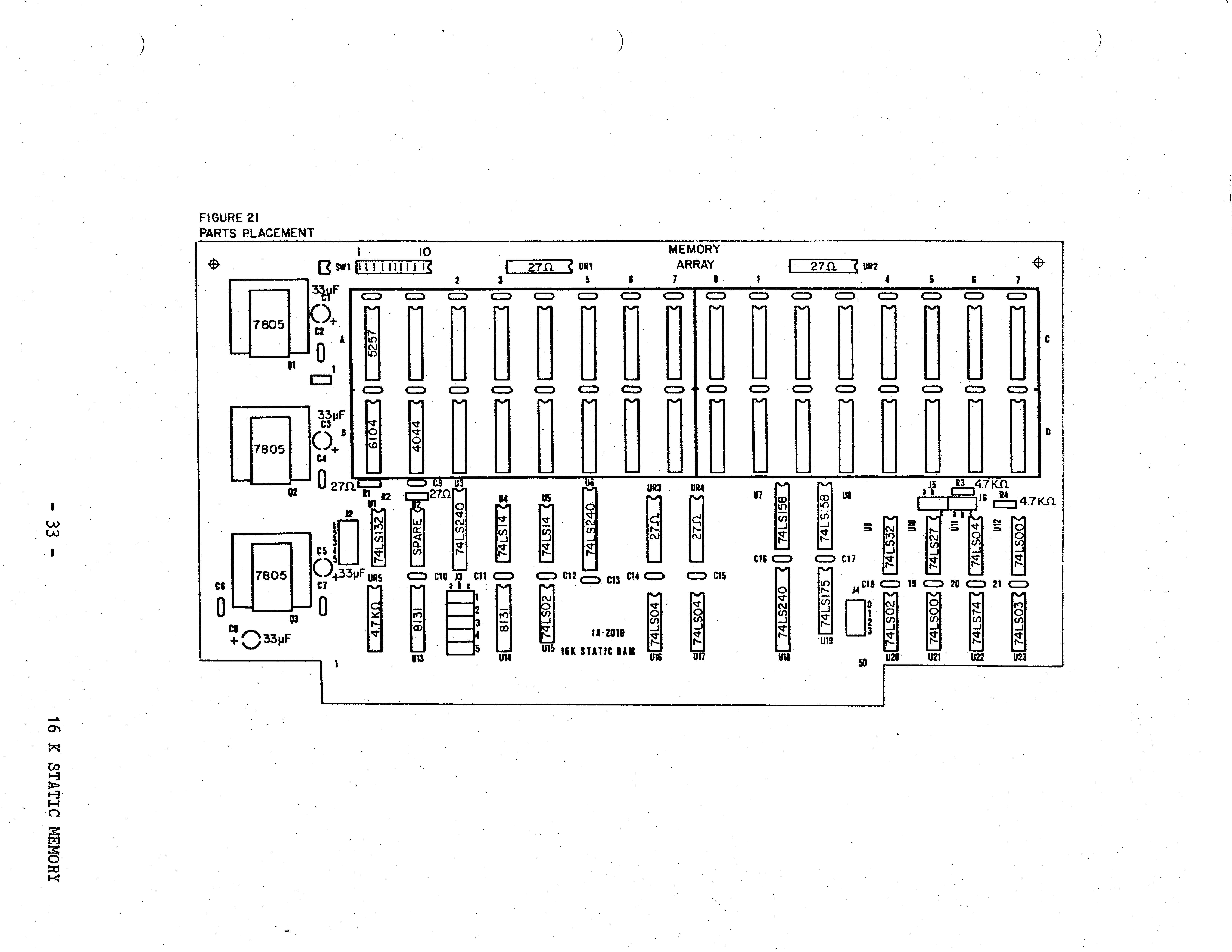
Here's a PDF of the Ithaca IA-2010 Rev 0 manual. It includes a schematic (dated Aug 1979) and a PC board layout. The layout looks very similar to the Rev A boards shown above. For convenience, here's a horizontal view of the board layout from the Rev 0 manual.
In 2020 I was asked for docs for the IA-2010 and supplied them. My customer then informed me about differences between the docs and the board they had in hand. The image of the assembled board above is from that customer. Here's what was said. - Herb
"Hi Herb, thank you, was able to download the manual. Do you know this board? On my board are more jumpers than described in the manual. In the upper left corner is a rocker switch, and beside the J5 is a J6, both are not described [in the manual]. I tested the board in an IMSAI with an original 8080 MPU board. Only the CPU and the RAM board are in the system.
"But I am only able to address two memroy locations, every even and every odd memory position shows the same content. On the odd positions (on all 16K) are always bit 0/1/7 on. The memory chips are all ok, tested this chips with a B&K Precision 575A. If you have advice I would be very happy, I would like to use such a nice board in my IMSAI."
I responded as follows but now with 2025 corrections by me in []'s:
The sketched figure of the circuit board layout in the manual, has some object to the left of "SW1" the long DIP switch in the upper left corner. I see J5 and J6 designations in the same layout, on the far lower right just below the DRAM array.
In the schematic, J5 switches an "error" signal from bus pin 98. I'd see how that bus signal works on your system. In the manual, page 36 in the appendix describes J5. [No, page 36 does *not*.]
In the schematic, J6 is the jumper on the output pin 5 of flipflop U22 74LS74. Page 10 of the manual has another sketch of the board and indicates J6 as "error line enable". Possibly on your [rev A] board, that's now J5. [I'm not sure now if the error signal is on PC board J5 or J6.]
[Schematic J6 selects the logic driving the "page 1" and "page 0" signals. But Appendix II page 36, again the Rev 0 manual, describes "A0 polarity" and references "an unlabled jumper ... directly to the left of J5". The Rev 0 schematic, shows an A0 jumper (IC 11 pin 12). The lable "J4" refers to the wait-state jumpers below, not the ABC jumper above. And on the Rev A board, J5 is directly to the left of J6. I believe the "unlabled jumper" for A0 may now be labled J5, and the schematic J6 is labeled J6 on the Rev A board.]
I suggest using your ohmmeter to verify J5 and J6 on your board, match or not what's on the schematic. I don't recall a general use of S-100 pin 98 for "errors". You might see if the Ithaca Intersystem Z80 board (details later in this email) accepts that signal and so determine any utility for it for your IMSAI 8080. My guess, is "no".
[I should have told this person, look at the A0 and Page 0/1 switching. It likely accounts for their odd/even data problem.]
I don't see references [in the manual] to a [small] header or DIP switch immediately next to the "top" voltage regulator. This will need to be resolved the hard way. You will have to use an ohmmeter and your eyes, to trace the lines from that DIP switch to their logic IC connections, and then determine what those are [or should be] on the schematic.
[The 10-position DIP switch on the top right of the board, is the "board address select switches". Manual pages 11 through 13 describe their settings, and the schematic shows the 10 switches as two "SW1" 5-switch pairs, off IC's 14 and 15. The schematic shows nearby, five "J3" abc jumpers; the physical PC board has a set of five jumpers near the S-100 edge connector. In 2025 I can't find on the schematic, references to a set of two switches. ]
There's also in your photo, a two-pin header between the top two regulators, which is open in your photo. Same prescription: trace with ohmmeter and eye.
After doing that, could you please inform me of the details? If you choose to draw/redraw a schematic, that would be very informative. I will with your permission, add your photo and your details to my manual. I don't know or recall, if you have done this kind of work before. But this was common work in the era, to update one's documentation. - Herb
I don't have further correspondence. So this is still unresolved. In 2025 I"ve reviewed the documents and photos and added my updates with [] remarks. - regards Herb Johnson
This page is copyright Herb Johnson (c) 2025. Some content on this page, belongs to the authors so named, and is used with their permission. Contact Herb at www.retrotechnology.com, an email address is available on that page..